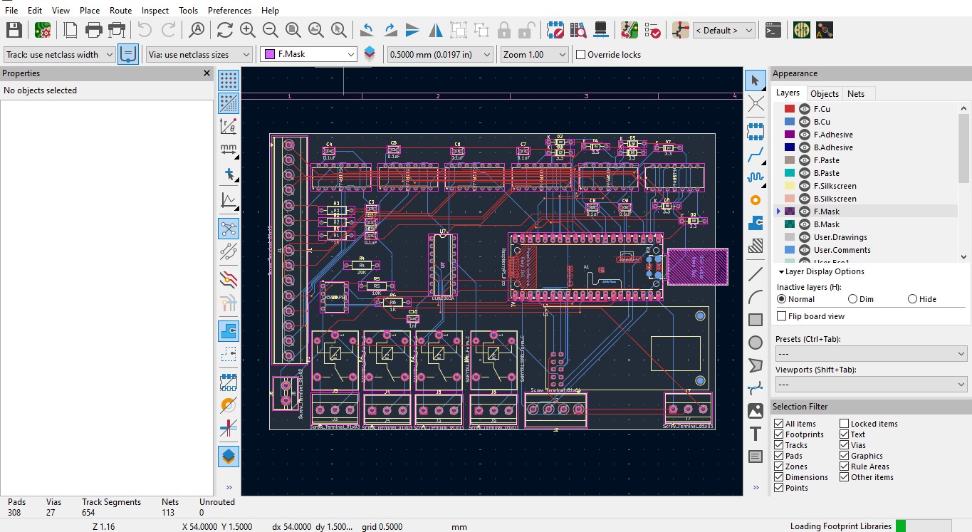
3 Electronics Design Package

PCB Design

FROM SCHEMATIC TO MANUFACTURING

Learn professional PCB development using KiCad. Build skills in schematic capture, component libraries, PCB layout, multilayer routing, design verification, manufacturing files and practical electronics projects.

Three Learning Levels KiCad-Based Training Manufacturing Workflow
Training Mode

Online and Offline

Core Skills

Schematic and PCB Layout

Certification

Professional Certificate

Batch Options

Regular and Weekend

PCB design training
SCHEMATIC → PCB → GERBER Complete PCB development workflow

Design Professional Electronic Circuit Boards

The PCB Design package covers the complete process of converting an electronic circuit concept into a manufacturing-ready printed circuit board.

Students learn component selection, schematic capture, footprint management, board placement, routing, design-rule checking, three-dimensional inspection and fabrication-file generation.

  • Read electronic schematics and component datasheets
  • Create professional KiCad schematics
  • Develop symbols and footprints
  • Route single-layer, double-layer and multilayer boards
  • Prepare Gerber, drill and bill-of-material files
Three Levels — One Great Career

Select Your PCB Design Level

Begin with electronics and KiCad fundamentals, advance to custom libraries and two-layer boards, and complete the Professional level with multilayer design and an industrial project.

Level 1

Basic

Recommended duration: 6–8 weeks

  • Electronics Fundamentals
  • Reading Circuit Diagrams
  • KiCad Introduction
  • Schematic Capture
  • Basic Single-Layer PCB Layout
Course Fee ₹7,500
Apply for Basic Level
Level 2

Intermediate

Recommended duration: 8–12 weeks

  • Custom Schematic Symbols
  • Footprint Creation
  • Two-Layer PCB Design
  • ERC and DRC
  • Three-Dimensional PCB Viewer
Course Fee ₹13,500
Apply for Intermediate Level
Level 3

Professional

Recommended duration: 12–16 weeks

  • Multilayer PCB Design
  • High-Speed Routing Basics
  • EMI and EMC Fundamentals
  • Gerber, Drill and BOM Files
  • Industrial PCB Design Project
Course Fee ₹21,000
Apply for Professional Level
Software and Skills

Technologies Covered

Learn the software, design methods and production deliverables used throughout a professional PCB workflow.

KiCad

Schematic capture, PCB layout and library management.

PCB Routing

Placement, track routing, vias, planes and multilayer boards.

3D Verification

Inspect board shape, components and mechanical clearances.

Manufacturing

Gerber, drill, BOM and assembly documentation.

Practical Applications

PCB Projects You Can Learn to Develop

Apply your skills to useful electronic, automation and embedded-system circuit boards.

Power Supply PCB

Design regulated power-supply and protection circuits.

Controller Board

Develop microcontroller, sensor and communication boards.

Automation Interface

Create relay, driver and industrial interface circuits.

IoT Hardware

Design connected boards for monitoring and remote control.

Learning Methodology

Learn Through the Complete PCB Workflow

01

Understand the Circuit

Study components, datasheets and circuit functions.

02

Draw the Schematic

Create logical circuit diagrams and verify connections.

03

Design the PCB

Place components and route tracks according to design rules.

04

Prepare Manufacturing Files

Generate verified Gerber, drill and assembly documents.

Eligibility

Who Should Join?

Diploma Students

Electronics, electrical, instrumentation and related branches.

Engineering Students

Learners seeking practical electronics and hardware-design skills.

Embedded Developers

Students building robotics, IoT and controller projects.

Working Professionals

Technicians and engineers upgrading PCB-development skills.

Frequently Asked Questions

Course Information

Yes. Beginners should begin with the Basic level, which introduces electronics, circuit diagrams, KiCad and simple PCB layouts.

Yes. KiCad is used for schematic capture, symbol and footprint creation, PCB layout, three-dimensional viewing and manufacturing files.

Practical exercises and projects are included according to the selected level, available equipment and current batch plan.

A CTI course-completion certificate is issued after completing the required classes, practical work and project assessment.

Start Your PCB Design Career

Choose your learning level and submit the CTI online admission form. Our admission team will contact you regarding the next available batch.

Apply Now